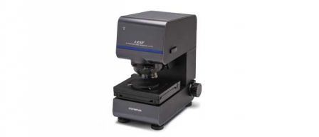
Microscopic shape measurement using a laser microscope
1. Application
Transparent materials are used in various manufacturing processes for electronic equipment, semiconductors and electronic components, and basic research. One common application is to measure the height (step) of a film from the glass substrate to which the transparent film has been applied. Because the thickness of a coated film greatly affects the performance and functionality of the resulting product, it is important to measure the thickness of the film after it has been applied to make sure it is the correct height.
Measuring the height of a transparent film has long been a challenge. Using an optical microscope to evaluate the surface profile of a film is difficult because the film’s transparency makes it very difficult to focus. In addition, since the materials are non-conductive, it is also difficult to observe the film using an electron microscope, which requires a metal film to be deposited on the surface. Contact-type step testers are also problematic because the stylus can damage the surface of the film.
2. The Olympus solution
With the LEXT 3D laser scanning microscope, the reflected light focused by the confocal optical system can be extracted so that even the reflection from a transparent film surface with low reflectivity can be captured by the high-sensitivity detector. Most importantly, the microscope uses laser light to enable reliable non-contact surface profile measurements without damaging the sample.
Images
(1) Step of one transparent film layer : 7.095 μm

(2) Step of one + two transparent film layer : 28.819 μm

(3) Step of one + two + three transparent film layer 36.739 μm


