Evident LogoOlympus Logo
Olympus Industrial Resources
Application Notes
Back to Resources

Au Area Ratio Measurement for Bonded Surfaces after Bump Abruption


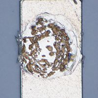
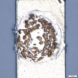
Au remaining on the bonding surface after bump separation_ob50×z4×_BF
Au Bump

1. Background

As package miniaturization and space-reduction technologies enhance overall product performance in contemporary electronic devices, Flip-Chip Bonding (FCB) – characterized by a small mounting footprint and reduced wiring distance – applications are increasing.

2. Application

Flip-Chip Bonding involves the bonding of on-chip electrodes to printed circuit board (PCB) electrodes through Au bumps. Without incorporating additional wiring, the bond strength directly influences the circuit’s conductivity. Since bond alloying contributes to reinforced bond strength, measuring the area ratio of non-alloy Au electrodes enables inspectors to confirm the degree of bond between the bump and the circuit board.

3. The Olympus solution

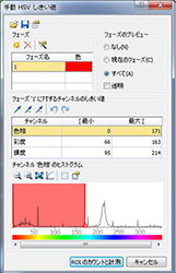
The Olympus DSX1000 digital microscope achieves resolutions comparable to state-of-the-art optical microscopes through the incorporation of high-NA/low-aberration field lenses. Extended Focal Image (EFI) technology allows users to acquire clear imagery across the entire field, even for difficult-to-focus surface configurations. Acquired images are directly transmitted via OLYMPUS Stream software for measurement. Users may further refine the measurement area through HSV settings.

Au remaining on the bonding surface after bump separation_ob50×z4×_BF_ROI

Brightfield Imagery: 50X field lens with 4X zoom

Au remaining on the bonding surface after bump separation_manual

Manual HSV threshold settings

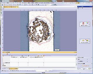
Au remaining on the bonding surface after bump separation_ob50×z4×_BF_ROI_Count and Measure

ROI designation / measurement result
Olympus IMS

Products Used for This Application

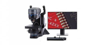
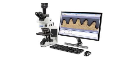
Better images and results. DSX1000 digital microscopes enable faster failure analysis with accuracy and repeatability.

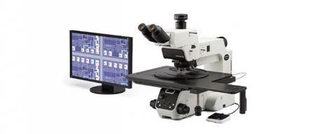
The MX 63 and MX63L microscope systems offer quality observations for 300 mm wafers at largest, flat panel displays, print circuit boards, and other large samples, featuring the versatile functions and ergonomic, user-friendly designs. The flexible module design provides optimal observation systems for diverse inspection purposes. By the combination with OLYMPUS Stream image analysis software, your inspection procedure from observation to report generation can be simplified and streamlined.
Stream Enterprise software with integrated data management offers intelligent step-by-step workflows to acquire sharp, crisp images that are ready for quantitative measurements and professional reporting based on the latest standards.
Sorry, this page is not available in your country
Let us know what you're looking for by filling out the form below.
Sorry, this page is not available in your country