Executive Summary
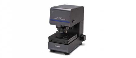
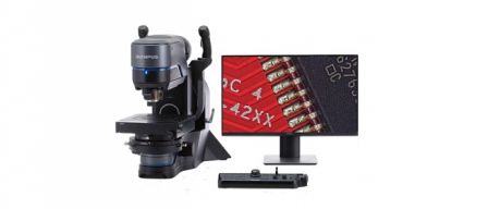
Driving the global spread of renewable solar energy, French company S’Tile is developing an innovative solar cell, saving on manufacturing costs and enhancing performance compared to conventional designs. Known as the i-Cell, this device consists of four thin subcells interconnected in series on an integrated silicon substrate. Through utilizing a low-cost sintered silicon support, this saves on precious materials and leads to cost savings of 30%, while the subcell format reduces electrical resistive losses. The manufacturing process involves many steps, each of which must be carefully and individually optimized for maximizing solar cell performance, and the Olympus DSX500 and LEXT OLS4100 have proved instrumental in optimizing i-Cell fabrication.
Introduction
Sustainable energy sources are set to contribute increasingly towards our ever growing global demands. However, solar cell construction is expensive, demanding energy-hungry manufacturing procedures and precious materials. Minimizing the consumption of these materials therefore drives down costs while lessening environmental impact, breaking down the barriers to the widespread generation of unlimited clean, green, solar energy. Working towards this goal is S’Tile, a spin-off company from the University of Poitiers (France). Founded in 2007, S’Tile has invented a new type of solar cell to improve the costperformance ratio. Teaming up with Olympus, the company has employed high-resolution digital light microscopy with the Olympus DSX500, and LEXT OLS4100 confocal laser scanning microscope for a new way to investigate the solar cell. This new generation of digital light microscope merges sophisticated imaging techniques with a user-friendly interface, enabling S’Tile engineers to quickly and efficiently inspect a range of features, from porosity to surface texture in unprecedented detail. Engineer at S’Tile, Francois Chancerel discusses how digital light microscopy has been instrumental in facilitating the optimization of fabrication processes central to enhancing S’Tile’s proprietary solar cell design – the i-Cell.
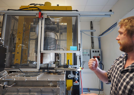
Figure1: Francois Chancerel presenting an inductive heating hot press specially designed by S’Tile for silicon sintering.
It can produce up to 235mm round sintered wafers.
The i-Cell – low cost, high efficiency
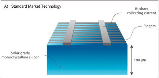
The application of solar cell technology depends on cost versus energy efficiency (i.e. the percentage of light transformed into electricity), and the i-Cell (Figure 2) minimizes this ratio through several approaches:
- Photon-harvesting layer is composed of only a very thin layer of p-type monocrystalline silicon (MonoSi)
- Low-cost silicon supporting solar-grade layer protects against breakages, reducing cost compared to conventional solar cells with thick solar-grade silicon layers
- Reduced size of metallic contacts decreases silver use by half and copper by 90%
- Four sub-cells connected in series lowers current and increases voltage through electrodes, improving energy efficiency thanks to reduction of resistive losses during module integration. Commercially viable efficiencies of over 18% have now been achieved with the i-Cell, and this
 |
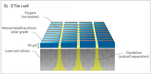 |
Figure 2: The S’Tile i-Cell solar cell design. |
Process optimization in i-Cell fabrication
The fabrication process of the i-Cell dictates the cost-performance ratio, and this involves several steps, as explained below:
1. Substrate fabrication
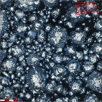
Figure 3: Silicon powder inspection guides sintering conditions. | The substrate is produced through sintering of low-grade silicon powder. On applying heat and pressure, sintering produces a dense layer from a powder, and this process is highly dependent on grain size and morphology of the silicon powder. S’Tile previously relied upon laser granulometry to determine the size and distribution of grains. This is fast, but does not provide information on grain morphology – only the average size and distribution. A complementary approach, microscopy instead allows the visualization of geometry, facilitating inspection (Figure 3). “We used the granulometry software,” says Mr Chancerel, “Olympus helped us in correcting our sample preparation protocol, and with the sample analysis software to separate grain boundaries.” |
2. Inspecting the conductive wells in the substrate
3. Layering
4. Reducing reflection through surface texturisation
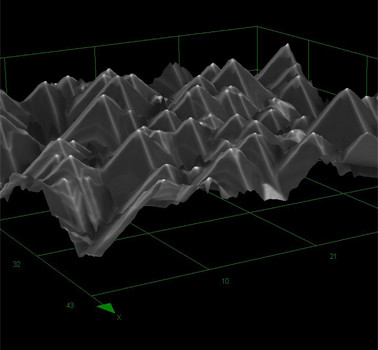 Figure 6: Measuring surface texture for reducing reflection. High-resolution characterization is achieved even through the antireflective coating with the LEXT OLS4100 3D confocal laser scanning microscope, assessing the texturisation process and reducing light reflection. | When light hits a flat silicon surface, approximately 30% is reflected instead of absorbed. Minimizing reflectivity is vital for solar cells and is achieved through two means: surface texturization, and an extra anti-reflective layer. With its high resolution imaging capabilities, confocal laser scanning microscopy lends itself to measuring surface features such as these, and S’Tile employed the Olympus LEXT OLS4100 3D measuring microscope for this purpose. The pyramid morphology of the surface (Figure 6) reduces reflection, capturing and continually re-reflecting light between each pyramid. Height, shape and distribution are all important, and can be optimized through fabrication. Mr Chancerel explains: “We tested different protocols, and compared the success of each based on surface texture using standard widefield light microscopy. However, with the height differences being in some cases just one micron, the limited resolution meant this was not possible.” The LEXT was subsequently employed for this task, he goes on to comment: “Achieving this quality of images with a light microscope is new to us, and they are comparable to electron microscopy. We found it impressive to use the LEXT.” Combining an optimized surface texture with an anti-reflection layer, it is possible to reduce reflection to 5 or 10%, maximizing energy efficiency. |
5. Engraving
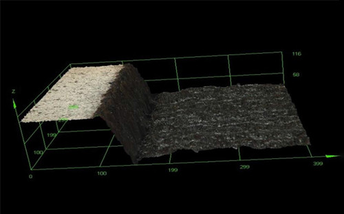 Figure 7: Well shape and surface integrity inspected after laser engraving. High-resolution 3D imaging with the DSX500 enables inspection of well morphology and surface integrity, optimizing laser engraving parameters and avoiding surface damage. | To form the network of electrodes overlaying the MonoSi surface, laser scribing creates channels in the silicon to be filled with silver. Inspecting this process, it is important to collect information on a variety of aspects. Well shape and depth dictate electrode morphology, and therefore resistance. In order to change the width and depth, a variety of different parameters can be controlled with laser scribing, such as wavelengths and intensity. “Previously, with the 2D microscope, we were unable to produce 3D images, and although we could inspect the depth of the wells, we could not perform this completely along the wells for a complete picture, like we now can with the DSX500 [Figure 7].” It is also important to inspect surface integrity, as a smooth surface is required for fabricating the interconnections between subcells. Since the laser parameters can also be modulated for the smoothest surface, it is vital to know if the laser is damaging the silicon, and it can be seen quickly and directly with the DSX500 if the surface is damaged. |
6. Metallization & firing
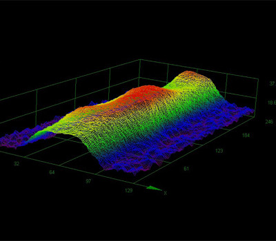 Figure 8: Inspecting electrode grid morphology. Height and width of the finger grid can be modulated from screen printing optimization to minimize resistive and optical losses. Inspecting the metallization helps guide this process, using the DSX500 3D analysis software at 100x magnification. | The metallization of adding silver into the engraved channels is performed using screen printing, and the form of the electrodes has a significant impact on solar cell efficiency. Mr Chancerel explains: “A larger surface area minimizes resistive losses, but a really thin strip maximizes the surface area of the photon-harvesting silicon.” Screen printing has many parameters to control, and to guide the process optimization, 3D images of the silver electrodes were captured and analyzed with the Olympus DSX500 (Figure 8). “The height mapping function is highly accurate, providing a comprehensive view instead of individual points. We can measure volume, average surface area and minimum surface area, enabling us to judge the quality of a metallization protocol.” “The DSX has really helped advance our metallization process. We previously had to analyses cross-sections, and so were limited to testing final samples, only finding the best printing and firing combination. With 3D analysis of printed samples, we can separate the steps and easily optimize each step individually.” |
Summary
Solar cell technology is well established, and the primary goal is now to bring down manufacturing costs while increasing efficiency, making this renewable energy source more accessible. The work of S’Tile on its i-Cell design is proving instrumental in this trend, and the company is fast approaching a market-ready design. “Alongside efficiencies of 20%, the second goal is to attain manufacturing costs 30% lower than conventional designs. Now we are interested in industrial collaborations to help us reach these targets.” Digital light microscopy with the DSX500 and LEXT OLS4100 enables fast and efficient inspection after every process, alongside more specialized methods. Mr Chancerel comments: “We can now understand much more clearly why one protocol leads to better results, and our different measurement tools fit together to guide the complete process optimization.”
Researcher Information
François Chancerel works as R&D Engineer at S’Tile, a research focused spin-off company dedicated to the further optimization of solar cells, located in Poitiers, France.
Email: contact@silicontile.fr
