La fabricación de semiconductores es un proceso polifacético e intrincado que cubre numerosas etapas, donde la precisión es primordial y la innovación es la fuerza impulsora. Su grabado representa una etapa crucial en el proceso de producción, ya que es fundamental para definir los patrones complejos y las estructuras esenciales para los dispositivos electrónicos modernos.
A lo largo de este artículo, se expone el proceso de grabado de forma más detallada y una forma más sencilla de controlar el espesor de los revestimientos de las cámaras de grabado.
¿Cómo funciona el grabado en la fabricación de semiconductores?
El grabado es un método que se emplea en la fabricación de semiconductores para eliminar selectivamente capas de material a partir de un sustrato, como una oblea/placa de silicio, con el fin de crear patrones y estructuras. Este proceso se lleva a cabo en cámaras de grabado: entornos controlados donde las obleas/placas semiconductoras se exponen a agentes de grabado (químicos o plasmas que eliminan selectivamente material a partir de la superficie de la oblea). Las cámaras de grabado están diseñadas para mantener una temperatura, presión y concentraciones químicas precisas con el objetivo de garantizar un grabado uniforme y exacto en toda la oblea.
Durante el proceso de grabado se requerirán revestimientos especiales dedicados tanto a proteger los componentes de la cámara de los agentes corrosivos como a mejorar el rendimiento del proceso. El itrio es adecuado para estas aplicaciones debido a su excepcional resistencia química, estabilidad térmica y compatibilidad con materiales semiconductores. Estas propiedades aseguran la larga duración de las cámaras de grabado y contribuyen a una fabricación homogénea y fiable de dispositivos semiconductores.
El control de espesor del itrio surge como un desafío crítico que exige atención meticulosa y soluciones avanzadas.
Cuatro razones para controlar el espesor del itrio en la fabricación de semiconductores
En el proceso de grabado de la fabricación de semiconductores, controlar el espesor del itrio es importante por varias razones, entre ellas:
1. Control del proceso
El espesor del revestimiento de itrio afecta directamente el rendimiento de la cámara de grabado. Al controlar el espesor, los ingenieros pueden confirmar que la cámara funciona dentro de los parámetros específicos, lo que optimizará la etapa de grabado y mantendrá una calidad constante del producto.
2. Uniformidad
Confirmar que el espesor del itrio es uniforme alrededor de todas las paredes de la cámara de grabado es determinante para lograr resultados de grabado uniformes.
3. Prevención para evitar la degradación del revestimiento
Con el tiempo, los revestimientos de itrio pueden degradarse debido a factores como el ataque químico o los ciclos térmicos. El control de espesor permite detectar de forma temprana debilitamiento o degradación en el material; esto actúa como un mantenimiento antes de que el revestimiento se vea comprometido. Además, favorece la vida útil de la cámara de grabado prolongándola y reduciendo su tiempo de inactividad.
4. Rentabilidad
El control de espesor regular del itrio favorece un mantenimiento y renovación proactivos, en lugar de reparaciones o reemplazos reactivos. El ahorro de costo(e)s es tangible, ya que se evitan tiempos de inactividad inesperados y la vida útil de los componentes de la cámara de grabado se ve prolongada.
Tecnología XRF portátil para controlar con exactitud el espesor del revestimiento de itrio
La tecnología de fluorescencia de rayos X (XRF) en modo portátil se distingue por ser una forma sencilla de controlar el espesor del revestimiento de itrio de las cámaras de grabado.
Los analizadores XRF portátiles emplean rayos X con el fin de facilitar análisis in situ de materiales, sin dañar las muestras. Este método de ensayo no destructivo es apropiado para controlar la calidad en la producción de semiconductores, ya que el analizador mide el espesor del revestimiento de itrio sin comprometer la integridad de la cámara de grabado o la muestra semiconductora.
Encima, el proceso es simple. El analizador emite rayos X que al incidir en el objeto bajo ensayo se convierten en rayos fluorescentes. El analizador detecta estos rayos X reflejados (secundarios) y usa los datos para calcular el espesor del revestimiento. Esto proporciona resultados de espesor en segundos. Conozca más sobre cómo medir el espesor de revestimientos a través de nuestra publicación de blog: En las buenas y en las malas: uso de la XRF para medir el espesor del revestimiento.
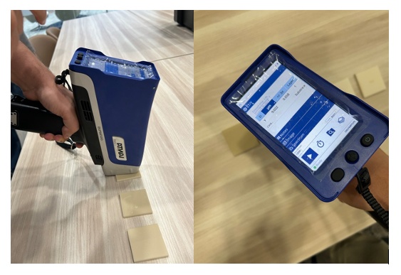
Técnico midiendo el espesor del revestimiento de itrio con un analizador XRF portátil Vanta™
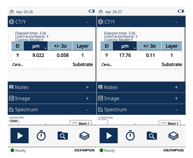
Resultados del espesor del revestimiento de itrio (Y) en la pantalla de un analizador XRF portátil Vanta
Nuestros analizadores XRF portátiles, gracias a algoritmos avanzados y procedimientos de calibración, otorgan medidas precisas del espesor del revestimiento de itrio en solo unos segundos.
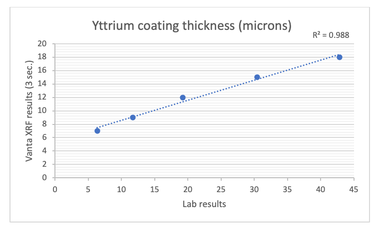
Los resultados de espesor del revestimiento de itrio, obtenidos con el analizador XRF portátil Vanta, coinciden de cerca con las medidas de laboratorio.
Por otra parte, los analizadores XRF portátiles también son dispositivos versátiles. Pueden medir el espesor del itrio a través de una amplia gama de materiales y otros tipos de revestimiento. Su diseño compacto y fácil de usar los convierte en los instrumentos idóneos para las mediciones in situ, ya que permiten a los técnicos ejecutar controles de calidad con facilidad y eficiencia.
Si desea obtener más información sobre las mediciones de espesor para revestimientos con el analizador XRF portátil, póngase en contacto con nuestro equipo para formularnos cualquier pregunta o concertar una demostración.
Contenido relacionado
De grueso a fino: Tecnología XRF para medir el espesor de revestimientos
¿Cómo hacer para agregar el modelo Revestimiento a su analizador Vanta?