Executive Summary
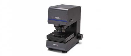
Dr Megan Cordill from the Erich Schmid Institute for Materials Science of the Austrian Academy of Sciences and the Department of Material Physics at the University of Leoben (Austria), has been researching thin films on polymer substrates for flexible electronic applications. Coupling a mechanical straining stage with high-resolution observation allows in situ analysis of electrical and mechanical properties. As an alternative to atomic force microscopy (AFM), integrating the Olympus LEXT OLS4100 confocal laser scanning microscope proved to be faster with a wider field of view, and allowed the measurement of a wider range of height features. Significantly, the work provided evidence to illustrate the damaging effects promoted by the inclusion of a chromium or tantalum adhesion layer.
Introduction
This case study explores how the application of confocal laser scanning microscopy with the Olympus LEXT OLS4100 is facilitating the different aspects involved in the development of flexible electronic devices. With the electronics industry rapidly moving towards flexible, lightweight devices, there are many factors to consider in designs that are both robust with a long life expectancy. Manufacturing electronic devices on deformable polymer substrates is the key characteristic of these technologies, and one approach to design is overlaying a thin layer of a conducting material on the polymer. Over the last five years, researcher Dr Megan Cordill from the Erich Schmid Institute for Materials Science and the University of Leoben (Austria), has been researching thin films on polymer substrates for new advanced thin film electronic applications. Linking electrical and mechanical properties under strain provides unprecedented insights into the behavior of thin film devices, and the depth of these insights is highly dependent on the observation technique employed for the in situ test. While Dr Cordill’s work has relied heavily on the high resolution afforded by atomic force microscopy (AFM), the introduction of the Olympus LEXT OLS4100 confocal laser scanning microscope into the laboratory has opened many doors for analysis.
Thin Film Behavior
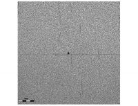
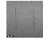
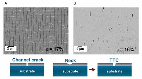
The research of Dr Cordill’s group looks specifically at the mechanical behavior of brittle and ductile materials under strain. She comments: “We are interested in the different layers – how they interact when they are stretched or bent. Too many different layers degrades both the electrical and mechanical behavior.” When the sample stretches under strain, materials behave differently. Brittle films such as hard metals break very easily with the formation of channel cracks, eventually delaminating from the underlying surface. Conversely, ductile films such as gold or copper are more complex, and instead exhibit plastic behavior. Initially, cracks extend from the surface (termed a ‘neck’). With increasing strain these may eventually develop into what are known as ‘through thickness cracks’ (TTCs), as shown in Figure 1. “We want to study how the microstructure of ductile films affects their electrical and mechanical behavior during mechanical loading, reflecting the strength and electrical resistance of the fi lm, as well as its adhesion to the substrate.” Interestingly, observing the sample after unloading masks any cracks, as the polymer substrate relaxes to compress the overlaying fi lm, and the sample may appear unaffected. Holding the sample for longer reveals any cracks, and therefore in situ testing is vital for visualizing deformation.¹ With the ability to measure delamination alongside electrical and mechanical properties in situ, the LEXT OLS4100 provides a comprehensive picture of thin fi lm behavior under loading conditions.
 |
|
Figure 1: Dr Cordill’s research into characterizing thin film behavior under mechanical loading.
Brittle (A) and ductile (B) films exhibit different behavior under mechanical load (ε ), forming channel cracks or necks that may develop into through thickness cracks (TTCs), as visualized with SEM. |
Electromechanical Testing of Ductile Films in Situ
The mechanical straining stage device coupled with the LEXT is controlled automatically for loading or unloading at a certain rate. Through coupling the device to the LEXT, this allows the measurement of sample displacement and the electrical resistance in parallel, and is therefore termed the ‘in situ squared’ method (Figure 2) by Dr Cordill’s group.
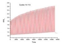
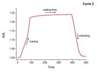
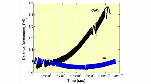
Cycles of straining replicate the fatigue the device would suffer outside of the laboratory. With the viscoelastic recovery of the polymer, after the sample is unloaded, it has a much lower resistance than it did at the maximum, and it is important to consider this alongside the maximum resistance (Figure 3). “Linking electrical and mechanical behavior is something we are able to do a lot better now with the LEXT and our testing device. We can stop at certain levels of strain, including a hold period of three minutes before acquiring the images.” This has proved beneficial in a range of studies. Dr Cordill’s group has found the LEXT provides information previously generated with the AFM, linking crack evolution as a function of strain. “With the AFM, we could only look at a small area – about 20–25 microns. Since the difference between a crack and a neck might only be fi ve microns, you’re looking at 4–5 cracks per image, which doesn’t provide meaningful statistics.” There is also the consideration of speed, and the AFM is slower, with one experiment taking one or two days.
“Compared to AFM I would say it takes half the time to learn how to run the LEXT system. Anyone can use an AFM, but to get high quality images, you need more experience, and it can be hard to inspect the same area each time. With the LEXT it is much easier to get it right the first time, as image acquisition is straightforward and intuitive.”
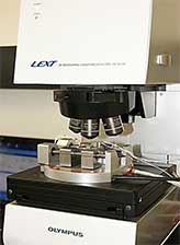
Figure 2: ‘In situ squared’ straining system with the Olympus LEXT OLS4100.
Load is applied automatically to a pre-determined value with known rate,
and sample displacement and electrical resistance is measured.
With the space of the LEXT stage, the standard 100x magnification working objectives can be used.
Layers – Less is More
With the research of Dr Cordill’s group, it is becoming increasingly clear that in certain film systems with certain microstructures, adhesion layers can prove detrimental to electromechanical behavior. For example, when a copper film has a chromium adhesion layer between the copper and the polymer, the sample is more prone to failure, compared to just a single copper film. In the rigid electronic industry it was historically thought that gold and copper have low adhesion to polymers, and so additional layers were introduced. Dr Cordill explains: “Although this was not the case looking back to the literature of the 1980’s, it was assumed that the interlayer would still be needed in the flexible electronic industry. Our work is instead showing that these interlayers are actually damaging.” For example, the chromium film has very low fracture strain and cracks form in this layer first. These subsequently act as a stress concentration point and cause cracks to form in the overlying copper layer – forming much faster than a film with just a copper layer (Figure 4). Without the chromium adhesion layer, after 100 cycles cracks are only just beginning to form.²
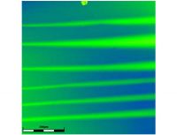
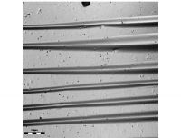
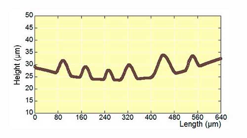
In contrast to copper, gold films can buckle and delaminate from the polymer substrate. On unloading the sample, these buckles form as the polymer springs back and the film becomes detached from the substrate. As higher loads are applied and removed, the buckles increase in size, or new buckles can form. Together with the film thickness, measuring the height and width with the LEXT calculates the adhesion energy of the metal and polymer interface. Figure 5 shows how the gold film with a tantalum adhesion layer delaminates from the polymer substrate. “Because we can see so many more buckles with the increased field of view compared with the AFM, I can make a lot of measurements just from one image. Actually, these buckles are too high for the AFM to measure.” Because of its higher range, the LEXT can be used to analyze a wider range of samples, and from these measurements, Dr Cordill’s research concludes that the adhesion of the gold layer is actually worsened in the presence of the tantalum adhesion layer.
Summary
Flexible electronic devices must withstand bending, stretching and twisting. The innovative work of Dr Cordill’s group has reinvented the design of flexible electronic devices, demonstrating how the inclusion of a chromium or tantalum adhesion layer is detrimental, leading to cracking in copper and buckling and delamination of gold films, respectively. Shedding light on the behavior of these devices in more detail than ever before, this discovery has been possible through coupling in situ testing with the fast and easy-to-use high-resolution imaging platform of the Olympus LEXT OLS4100. The LEXT provides a fast means to generating new information, especially when compared to AFM, where a wider dynamic range means samples with varying feature heights can also be investigated. “Manufacturers can now determine when cracks form, and respond to this information,” says Dr Cordill, who goes on to conclude: “Our approach is instrumental in guiding the optimization of materials and fabrication processes, leading us towards robust, market-ready devices.”
Researcher Information
Dr. Megan J. Cordill is working at the Erich Schmid Institute of Materials Science, Austrian Academy of Sciences, Department Material Physics, Montanuniversität Leoben; investigating the electro mechanical behavior of conductive films and flexible electronics.
E-mail: megan.cordill@oeaw.ac.at
References
- O. Glushko, et al TSF 552 (2014) 141 Glushko & Cordill, Experimental Methods (2014) in press
- Cordill, M.J. et al. (2010). Adhesion energies of Cr thin films on polyimide determined from buckling: Experiment and model. Acta Materialia 58; 5520–5531

