Microscope Solutions for
Semiconductor Manufacturing
- Home
- Microscope Solutions for Semiconductor Manufacturing
- Slicing and Polishing
Slicing and Polishing
Slice the ingot into thin silicon plates (wafers). Polish the top and bottom of the wafer surfaces. This flattens the surface so the circuit patterns can be imprinted. The polished wafer is then marked with laser marking equipment.
Inspecting the Surface Roughness of a Wafer
The wafer’s surface must be properly flattened to imprint precise IC patterns on it. As a result, detailed inspections of the surface roughness are required after polishing.
Our Solution
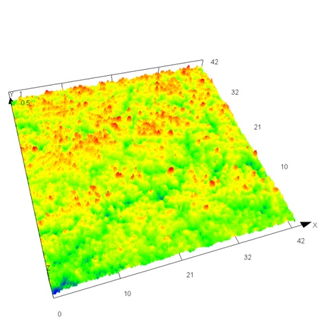
Our OLS series microscopes can show the surface roughness conditions of a wafer in fine detail after the surface polishing step. It can also measure the surface roughness at both the micro and nano level.
OLS series laser scanning microscope | Surface roughness of a wafer |
Application Notes
Explore related applications:
| |||
|
Confirm the Dimensions of the Water Mark
Each wafer has an identifying mark imprinted by a laser. As the size of the laser mark continues to become smaller (micron level), operators need precise inspection equipment that can measure its small dimensions.
Our Solution
Our OLS series microscope can finely represent the surface roughness conditions of a wafer after the surface polishing. It can measure surface roughness at both the micro and nano level.
OLS series laser scanning microscope |  Laser mark overview | Laser mark cross section |
Application Notes
Explore related applications:
| |||
| |||
|
