Semiconductor manufacturing is a multifaceted and intricate process encompassing numerous steps, where precision is paramount and innovation is the driving force. Etching stands out as a pivotal process stage during production, as it’s crucial for defining the intricate patterns and structures essential for modern electronic devices.
Here we explore the etching process in detail, highlighting an easy way to control the coating thickness of etch chambers.
How Etching Works in Semiconductor Manufacturing
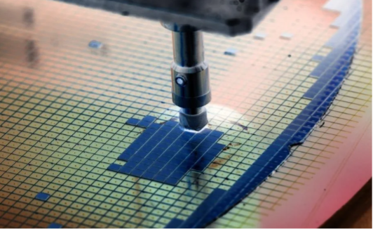
Etching is a method used in semiconductor manufacturing to selectively remove layers of material from a substrate, such as a silicon wafer, to create patterns and structures. This process takes place in etch chambers, controlled environments where semiconductor wafers are exposed to etchants—chemicals or plasmas that selectively remove material from the wafer surface. Etch chambers are designed to maintain a precise temperature, pressure, and chemical concentrations to help ensure uniform and accurate etching across the wafer.
Special coatings are necessary during the etching process to protect chamber components from corrosive etchants and to enhance process performance. Yttrium is well-suited for these applications due to its exceptional chemical resistance, thermal stability, and compatibility with semiconductor materials. These properties help ensure the longevity of etch chambers and contribute to consistent and reliable semiconductor device fabrication.
The control of yttrium thickness emerges as a pivotal challenge, demanding meticulous attention and advanced solutions.
4 Reasons to Monitor Yttrium Thickness in Semiconductor Manufacturing
In the etching process of semiconductor manufacturing, monitoring yttrium thickness is important for several reasons, including:
1. Process control
The thickness of the yttrium coating directly affects the performance of the etch chamber. By monitoring the thickness, engineers can confirm that the chamber operates within specified parameters, optimizing etching processes and maintaining consistent product quality.
2. Uniformity
Confirming uniform yttrium thickness across the etch chamber walls is crucial for achieving uniform etching results.
3. Prevention of coating degradation
Over time, yttrium coatings can degrade due to factors such as chemical attack or thermal cycling. Monitoring thickness enables early detection of thinning or degradation, enabling maintenance to be performed before the coating becomes compromised. This helps extend the lifespan of the etch chamber and minimize downtime.
4. Cost efficiency
Regular monitoring of yttrium thickness allows for proactive maintenance and refurbishment, rather than reactive repairs or replacement. This can result in cost savings by avoiding unexpected downtime and extending the usable life of the etch chamber’s components.
Portable XRF Technology for Precise Monitoring of Yttrium Coating Thickness
An easy way to monitor the yttrium coating thickness of etch chambers is through portable X-ray fluorescence (XRF) technology.
Portable XRF analyzers use X-rays to provide on-the-spot analysis of materials without damaging the sample. This nondestructive test method is well suited for quality control in semiconductor production, as the analyzer measures the thickness of the yttrium coating without compromising the integrity of the etch chamber or semiconductor sample.
Plus, the process is simple. The analyzer emits X-rays, and they strike the test object, causing it to fluoresce. The analyzer detects the returning X-rays and uses the data to calculate the thickness of the yttrium (Y) coating. This gives you thickness results in seconds. Read more about how coating measurement works in our blog post, Through Thick and Thin: Using XRF to Measure Coating Thickness.

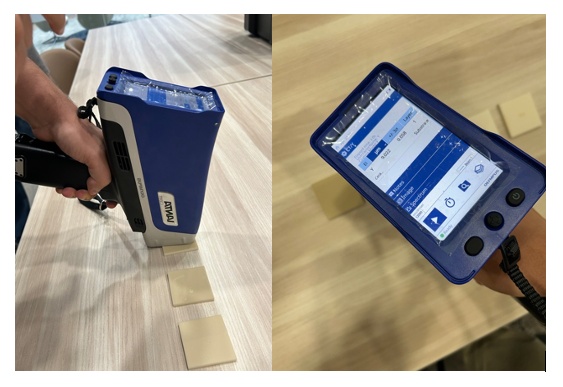
A technician measures yttrium coating thickness using a Vanta™ handheld XRF analyzer.
Yttrium (Y) coating thickness results on the screen of a Vanta handheld XRF analyzer.
With advanced algorithms and calibration procedures, portable XRF analyzers deliver precise measurements of the yttrium coating thickness in just a few seconds.
Vanta handheld XRF analyzer results for yttrium coating thickness closely match that of lab measurements.
Portable XRF analyzers are also versatile devices. They can measure yttrium thickness across a wide range of materials and coatings. Their compact and user-friendly design makes them ideal for on-site measurements, enabling technicians to perform quality control checks with ease and efficiency.
For more information about coating thickness measurements using portable XRF, reach out to our team with any questions or to set up a demo.
Related Content
Through Thick and Thin: Using XRF to Measure Coating Thickness

